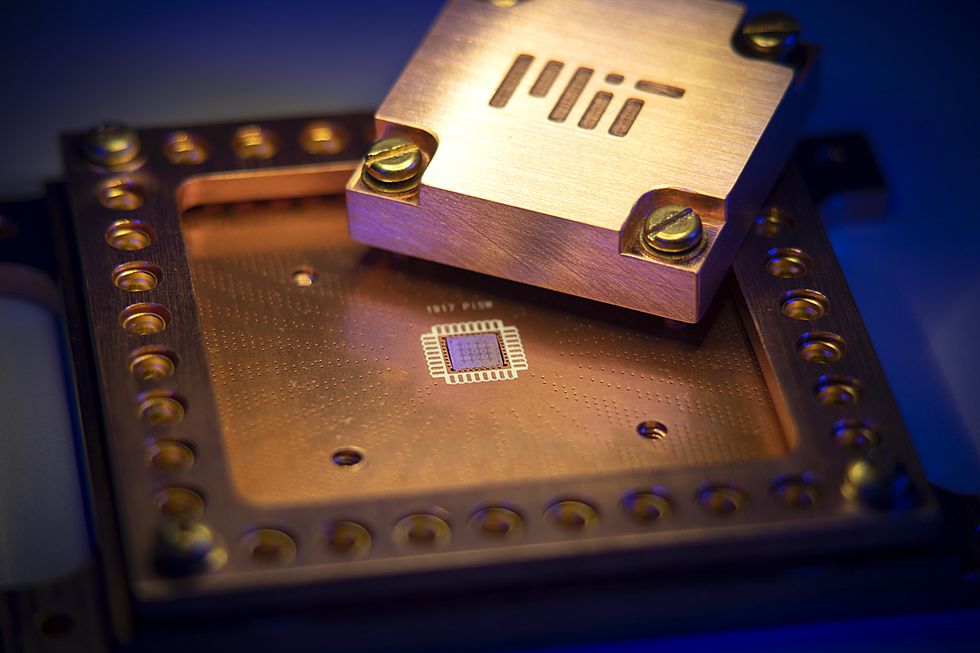
The race for quantum supremacy has reached a new level of complexity and commercial potential. While giants like IBM and Google advance their roadmaps for processors with over 1,000 qubits, the industry faces a formidable physical hurdle: component size. Currently, superconducting qubits are disproportionately large, requiring chips that can reach 50 millimeters or more, which hinders scalability and integration into compact systems. However, an innovation led by researchers at MIT (Massachusetts Institute of Technology) promises to transform this reality by using atomically thin materials to reduce qubit size by up to 100 times without sacrificing performance.
The Miniaturization Bottleneck and the 2D Solution
The central problem in superconducting quantum computing lies in the capacitors. To avoid signal loss and interference, current designs use coplanar capacitors, where the plates are positioned laterally on a silicon substrate. Although pure silicon minimizes defects, this configuration requires a vast surface area — approximately 100 by 100 micrometers per plate — to achieve the necessary capacitance. Multiplying this by thousands of qubits results in chips that are impractical for current cooling infrastructure.
The solution presented by MIT involves the transition to two-dimensional (2D) materials. The key component is hexagonal boron nitride (hBN), an atomic insulator that acts as the dielectric in a vertically stacked capacitor. Unlike conventional silicon oxides, which exhibit many defects at cryogenic temperatures, hBN is chemically inert and free of significant structural imperfections. By stacking layers of hBN between plates of niobium diselenide (another superconducting 2D material), researchers have managed to create extremely dense and efficient capacitors.
From Lab Bench to Industrial Viability
The transition of this technology to the industrial environment solves one of the biggest problems in quantum engineering: crosstalk. In dense chips, the electric fields of neighboring qubits often leak, causing computational errors. In MIT’s 2D sandwich design, about 90 percent of the electric field is contained within the capacitor structure. This allows qubits to be positioned much closer to each other, exponentially increasing processing density per square millimeter.
While the use of niobium diselenide presents challenges — such as instant oxidation upon contact with air — the research team developed fabrication protocols in controlled environments using argon gas. Once the layered structure is sealed, the component demonstrates long-term stability, even when exposed to the atmosphere. The next step for mass commercialization is the growth of these materials at the wafer scale, a technique already being explored by the semiconductor industry for next-generation transistors.
Economic Impact and the Future of the Hardware Market
The economic impact of this innovation is profound. Reducing the size of the quantum chip drastically lowers infrastructure costs. Quantum systems operate at temperatures near absolute zero (about 0.02 degrees above absolute zero), requiring massive and expensive dilution refrigerators. If a 1,000-qubit processor can be reduced from 50 millimeters to just a few millimeters, the demand for gigantic cooling systems decreases, allowing for more agile integration into existing datacenters.
Furthermore, the ability to manufacture high-performance, high-density qubits places companies that adopt 2D materials at a clear competitive advantage. As William Oliver, director of the Center for Quantum Engineering at MIT, stated, performance cannot be sacrificed for the sake of quantity. This new systems architecture ensures that scalability goes hand in hand with the fidelity of quantum operations. For investors and hardware sector players, the roadmap now points toward a convergence between 2D material nanotechnology and high-performance computing, signaling that the era of compact and powerful quantum computers is closer than previously predicted.
Official Announcement / Industry: Atomically Thin Materials Significantly Shrink Qubits via IEEE Spectrum.
About the Editorial Team
QOrigin Editorial is the science journalism core of QOrigin News, dedicated to transforming frontier academic research into in-depth analyses on quantum computing, physics, space exploration, and advanced systems architecture.